1. Solid Solution Strengthening (Material Process)
Old Answer
Solid Solution Strengthening
Large additions of chromium, molybdenum, and tungsten and smaller additions of tantalum, zirconum, niobium, and boron provide solid solution strengthening. The effects of solid solution strenghthening are stable and, conswquently, make the alloy resistant to creep, particularly when large atoms such as molybdenum and tungsten (which diffuse slowly) are used.
(Askeland,D.R,The Science and Engineering of Materials,3rd Edition, pg.402)
New, Better
In metallic materials, one of the important effects of solid-solution formation is the resultant solid-solution strengthening (Figure 10-7). This strengthening, via solid-solution formation, is caused by increased resistance to dislocation motion. This is one of the important reasons why brass (Cu-Zn alloy) is stronger than pure copper. We will learn later that carbon also plays another role in the strengthening of steels by formating iron carbide (Fe3C) and other phases (Chapter 12). Jewelry could be made out from pure gold or silver; however, pure gold and pure silver are extremely soft and malleable. Jewelers add copper to gold and silver so that the jewelry will retain its shape.
In the copper-nickel (Cu-Ni) system, we intentionally introduce a solid substitutional atom (nickel) into the original crystal structure (copper). The copper-nickel alloy is stronger than pure copper. Similarly, if less than 30% Zn is added to copper, the zine behaves as a substitutional atom that strengthens the copper-zinc ally, as compared with pure copper.

The effects of several alloying elements on the yield strength of copper. Nickel and zinc atoms are about the same size as copper atoms, but berylium and tin atoms are much different from copper atoms. Increasing both the atomic size difference and the amount of alloying elements increases solid-solution strengthening.
Recall from Chapter 7 that the strength of ceramics is mainly dictated by the distribution of flaws; solid-solution formation does not have a strong effect on their mechanical properties. This is similar to why strain hardening was not much of a factor in enhancing the strength of ceramics or semiconductors such as silicon (Chapter 8). As discussed before, solid-solution formation in ceramics and semiconductors (such as Si, GaAs, etc.) has considerable influence on their magnetic, optical and dielectric properties. The following discussion related to mechanical properties, therefore, applies mainly to metals.
(The Science and Engineering of Materials, Askeland D., Wright W., 384-385)
2. Closed-Loop Transfer Function (Control System)
Old Answer
Closed-loop transfer function: The closed-loop transfer function (CLTF) of any feedback control system can be determined by using a relatively straightforward process. We define R(s) as the input, C(s) as the output or control variable, G(s) as the forward path transfer function, H(s) as the feedback path transfer function, C(s) / R(s) as the Closed loop transfer function (CLTF), E(s) as the error signal, and B(s) as the feedback signal.G(s) includes all transfer functions and gains in the feedback path. ( Introduction to aircraft flight mechanics- Thomas R. Yechout, Steven L. Morris-page 399)New, better
In Figure 6.1, the transfer function from ys(s) to y(s) is called the closed-loop transfer function between ys(s) and y(s) because the loop is closed. Meanwhile, the transfer function from e(s) to y(s) is caled the open-loop transfer function because the loop is open. Consider the following to derive the closed-loop transfer functions. The closed-loop transfer function from ys(s) to y(s) is (6.1) when the signals of di(s) and d0(s) are zero:


Equation (6.2) is the closed-loop transfer function from di(s) to y(s) when the signals of ys(s) and d0(s) are zero:

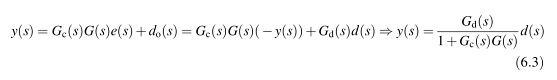
Equation (6.3) is the closed-loop transfer function from d(s) to y(s) when the signals of ys(s) and di(s) are zero:
By the superposition rule, the closed-loop transfer function from ys(s), di(s), d(s) to y(s) is

(Process Identification and Pid Control, Sung S., Lee J., 201-202)
Old Answer
Photo transistors:
These detectors produce electrical current proportional to input light intensity.
Phototransistors provide higher sensitivity (i.e., higher current) than do photodiodes but operate at much lower response times (milliseconds versus nanoseconds).
(Manufacturing: Design, Production, Automation and Integration Page 385)
New, better
4.2.5 Phototransistor (Semiconductor Device)
The phototransistor has a light sensitive, collector-base p-n junction which works on the principle of photodiode. THe photodiodes have small transparent windows that allow light to fall on the-n junction and electron-hole pairs are generated by the absorption of light energy in the form of photons.
The phototransistor is exposed to incident light through a lens opening in the transistor package. When there is no incident light, there is a small thermally generated collector-to-emitter leakage cureent. I,ceo; This is called the dark current and is typically in the nanoampere range. When light strikes the collector-base p-n junction, a base current I,b is produced that is directly proportional to the light intensity. This action produces a collector current which increases with I,b according to the relation, I,c=h,fe*I,b=b,dc*I,b. Except for the way the base current is generated, the phototransistor behaves as a conventional bipolar junction transistor. In many cases, there is no electr,cal connection to the base.
( First Course in Electronics Khan A., 130)
4.Robot-Human Charts (Robotics)
Old Answer
Robot-Human Charts
Robot-Human Charts originally prepared by Nof, Knight, and Salvendy are developed with two functions in mind, namely to aid engineers in determining whether a robot can perform a job and to serve as a guideline and reference for robot spesifications. The robot-human charts can also be useful in job design of combined systems, which integrate both robots and human operators. They contain three principal types of work characteristics.
1. Physical skills and characteristics, including manipulation, body dimensions, strength and power, consistency, overload, underload performance, and enviromental constraints.
2. Mental and communicative characteristics. The robot-human charts contain mental and communicative system attributes for robots and humans.
3. Energy considerations. A comparison of representative values of energy-related characteristics, such as power requirements, and energy efficiency for robots and humans.
(Manufacturing: Design, Production, Automation and Integration Page 272-274)
New, better
The concept of job and skill analysis was originated by Nof et al.(1980). This approach involves two sequential steps: Robot-Man Charts (RMC); and Job and Skill Analysis (JSA) method. The RMC procedure provides a means of identifying jobs which can be done either by robots or humans. Once it is determined that a robot can perform the job, JSA is conducted.
The RMC technique is a modification of the traditional man-machine charts used in motion and time study. It compares the relative abilities of humans and industrial robots in the following categories.
1. Action and manipulation: manipulation abilities (typical robot structures are polar robot, cylindirical robot, cylindirical moving robot and pick-and-place robot), bosy dimensions, strength and power, consistency, overload/underload performance, reaction speed and self-diagnosis.
2. Brain and control: computational capability, memory, intelligence, reasoning and signal processing.
3. Energy and utilies: power requirements, utilities, fatique/down-time/life expectancy and energy efficiency.
4. Interface: sensing and inter-operator communication.
5. Miscellaneous factors: environmental constraints, brain-muscle combination, training and social and phychological needs.
6. Individual differences.
(Human-robot interaction, Rahimi M., 8)
5.Serrated Chips(in Metal Machining)(Manufacturing)
Old Answer
Serrated Chips(in Metal Machining):
Serrated chips are semi-continuous in the sense that they possess a saw-tooth appearance that is produced by a cyclical chip formation of alternating high shear strain followed by low shear strain. This fourth type of chip is most closely associated with certain difficult to machine metals such as titanium alloys, nickel base superalloys, and austenitic stainless steels when they are machined at higher cutting speeds. However, the phenomenon is also found with more common work metals (e.g steels) when they are cut at high speed.
(Fundamentals of Modern Manufacturing: Materials, Processes, and Systems, Mikell P. Groover, p.492)
New, better
Along with the cutting speed increase, the serrated chip appears (Fig. 4b). Here the serrated type is not extremely obvious, but it indicates the production of important phenomenon namely the adiabatic shear occurs. This condintion is also called adiabatic shear critical state in cutting. It is generally considered that serrated chip is the representation of adiabatic shear in chips. According to the different degrees in adiabatic shear, the serrated chip may be divided into two types. One is the deformed band serrated chip (Fig. 4c) and the other is the transformed band serrated chip (Fig. 4d). Both have the essential differences in the forming conditions and the microscopic shapes. Certainly, the cutting condition is the decisive factor while the material does not change. But they have the same characteristic that adiabatic shear band (ASB) is produced between serrated chips.

(Advanced Design and Manufacture to Gain a Competitve Edge, Yan X., p. 191)
No comments:
Post a Comment